The 74HC595 is an 8-bit serial-in/serial or parallel-out shift register with output latches. Below are the specifications, application areas, and methods of implementing logic gate combinations using the 74HC595 IC:
Specifications:
- Manufacturer: Texas Instruments, NXP Semiconductors, etc.
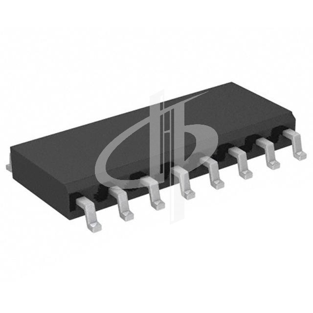
- IC Type: 8-bit Shift Register with Output Latches
- Package: DIP-16, SOIC-16
- Supply Voltage: 2V to 6V typically
- Output Current: 6-8mA typical
- Clock Frequency: 25 MHz typical
- Features: Serial Input, Serial or Parallel Output, Cascadable
Application Areas:
- LED Display Systems: Controlling multiple LEDs efficiently using serial communication.
- Digital Clocks: Utilized for driving segments of digital displays.
- Shift Register Applications: Serially transferring data to multiple outputs.
- Driving 7-segment Displays: Sequentially outputting data to drive 7-segment displays.
- IoT Devices: Useful for expanding output capabilities, e.g., driving various peripherals.
Implementing Logic Gate Combinations:
The 74HC595 can be used to implement various logic gate combinations. Here’s a basic example of implementing a logic gate with the 74HC595:
Example: Implementing an OR Gate
-
Logic Diagram:
-
Implementation Steps:
-
Connections:
- Connect the parallel outputs Q0 to Q7 of the 74HC595 to the inputs of the gates.
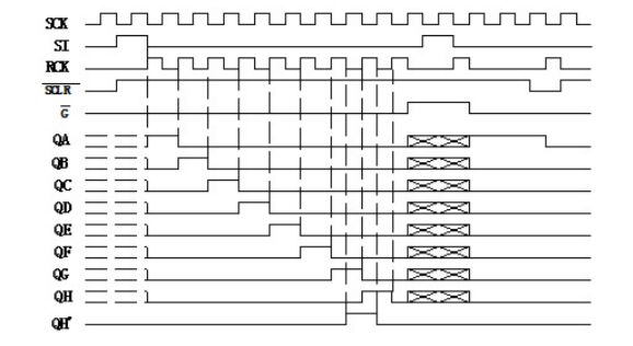
- Use the SER (Serial Input) and SRCLK (Shift Register Clock) inputs for shifting in data.
- Utilize the RCLK (Register Clock) to latch the outputs.
-
Data Loading:
- Load the required bit pattern to the shift register.
- Shift the data into the register by pulsing the SRCLK line.
-
Latching:
- Once the data is shifted in, pulse the RCLK line to latch the data to the output pins.
-
Output Interpretation:
- The output from the 74HC595 corresponds to the logic value obtained from the implemented gates.
-
By controlling the input data fed into the 74HC595, you can effectively emulate various logic gate behaviors. For OR gates, configuring the appropriate data pattern on the inputs and then latching the output can simulate the gate's functionality.
Note:
- The 74HC595 is a versatile component that can be cascaded to form longer shift registers or to expand the output capability of a microcontroller.
- Understanding the serial shift and latch operations of the 74HC595 is crucial for effectively utilizing its features in various applications.
Always refer to the IC's datasheet for detailed information on pin configurations, timing diagrams, and application guidelines when using the 74HC595 in your projects.